


Subsequent-Gen Graphics Memory Offers Sooner PAM3 Signaling & On-Die ECC
JEDEC on Tuesday revealed the official specs for GDDR7 DRAM, the latest iteration of the long-standing memory commonplace for graphics enjoying playing cards and completely different GPU-powered devices. The most recent know-how of GDDR brings a combination of memory functionality and memory bandwidth options, with the later being pushed primarily by the swap to PAM3 signaling on the memory bus. The most recent graphics RAM commonplace moreover boosts the number of channels per DRAM chip, supplies new interface teaching patterns, and brings in on-die ECC to maintain up the environment friendly reliability of the memory.
“JESD239 GDDR7 marks a substantial growth in high-speed memory design,” talked about Mian Quddus, JEDEC Board of Directors Chairman. “With the shift to PAM3 signaling, the memory commerce has a model new path to extend the effectivity of GDDR devices and drive the continued evolution of graphics and quite a few high-performance functions.”
GDDR7 has been in enchancment for only a few years now, with JEDEC members making the first disclosures throughout the memory experience a couple of 12 months previously, when Cadence revealed utilizing PAM3 encoding as part of their validation devices. Since then now we have heard from quite a lot of memory producers that we should all the time anticipate the last word mannequin of the memory to launch in 2024, with JEDEC’s announcement mainly coming correct on schedule.
As beforehand revealed, crucial technical change with GDDR7 comes with the swap from two-bit non-return-to-zero (NRZ) encoding on the memory bus to three-bit pulse amplitude modulating (PAM3) encoding. This variation permits GDDR7 to transmit 3 bits over two cycles, 50% additional data than GDDR6 working at an equal clockspeed. Due to this, GDDR7 may help better common data swap fees, the important half to creating each know-how of GDDR successively faster than its predecessor.
| GDDR Generations | |||||
| GDDR7 | GDDR6X (Non-JEDEC) |
GDDR6 | |||
| B/W Per Pin | 32 Gbps (Gen 1) 48 Gbps (Spec Max) |
24 Gbps (Transport) | 24 Gbps (Sampling) | ||
| Chip Density | 2GB (16GB) | 2GB (16GB) | 2GB (16GB) | ||
| Complete B/W (256-bit bus) | 1024 GB/sec | 768 GB/sec | 768 GB/sec | ||
| DRAM Voltage | 1.2 V | 1.35 V | 1.35 V | ||
| Info Worth | GDR | GDR | GDR | ||
| Signaling | PAM-3 | PAM-4 | NRZ (Binary) | ||
| Most Density | 64 Gb | 32 Gb | 32 Gb | ||
| Packaging | 266FBGA | 180FBGA | 180FBGA | ||
The first know-how of GDDR7 is anticipated to run at data fees spherical 32 Gbps per pin, and memory producers have beforehand talked about fees as a lot as 36 Gbps/pin as being merely attainable. However the GDDR7 commonplace itself leaves room for even better data fees – as a lot as 48 Gbps/pin – with JEDEC going so far as touting GDDR7 memory chips “reaching as a lot as 192 GB/s [32b @ 48Gbps] per machine” of their press launch. Notably, it’s a significantly better enhance in bandwidth than what PAM3 signaling brings by itself, which suggests there are a variety of ranges of enhancements inside GDDR7’s design.
Digging deeper into the specification, JEDEC has moreover as quickly as as soon as extra subdivided a single 32-bit GDDR memory chip into an even bigger number of channels. Whereas GDDR6 provided two 16-bit channels, GDDR7 expands this to 4 8-bit channels. The excellence is significantly arbitrary from an end-user’s perspective – it’s nonetheless a 32-bit chip working at 32Gbps/pin regardless – however it certainly has a considerable quantity of impression on how the chip works internally. Significantly as JEDEC has saved the 256-bit per channel prefetch of GDDR5 and GDDR6, making GDDR7 a 32n prefetch design.

GDDR Channel Construction. Distinctive GDDR6-era Diagram Courtesy Micron
The net impression of all of that’s that, by halving the channel width nonetheless retaining the prefetch dimension the similar, JEDEC has efficiently doubled the amount of data that is prefetched per cycle of the DRAM cells. This could be a pretty commonplace trick to extend the bandwidth of DRAM memory, and is definitely the similar issue JEDEC did with GDDR6 in 2018. Nevertheless it serves as a reminder that DRAM cells are nonetheless very gradual (on the order of a number of of MHz) and do not get any faster. So the one choice to feed faster memory buses is by fetching ever-larger portions of data in a single go.
The change inside the number of channels per memory chip moreover has a minor impression on how multi-channel “clamshell” mode works for better functionality memory configurations. Whereas GDDR6 accessed a single memory channel from each chip in a clamshell configuration, GDDR7 will entry two channels – what JEDEC is wanting two-channel mode. Significantly, this mode reads channels A and C from each chip. It is efficiently equal to how clamshell mode behaved with GDDR6, and it implies that whereas clamshell configurations keep supported on this latest know-how of memory, there aren’t one other suggestions being employed to boost memory functionality previous ever-increasing memory chip densities.
On that phrase, the GDDR7 commonplace formally supplies assist for 64Gbit DRAM devices, twice the 32Gbit max functionality of GDDR6/GDDR6X. Non-power-of-two capacities proceed to be supported as successfully, allowing for 24Gbit and 48Gbit chips. Help for greater memory chips further pushes the utmost memory functionality of a theoretical high-end video card with a 384-bit memory bus to as extreme as 192GB of memory – a enchancment that may little query be welcomed by datacenter operators inside the interval of huge language AI fashions. With that talked about, however, we’re nonetheless repeatedly seeing 16Gbit memory chips used on as we communicate’s memory enjoying playing cards, although GDDR6 helps 32Gbit chips. Coupled with the reality that Samsung and Micron have already disclosed that their first know-how of GDDR7 chips may even prime out at 16Gbit/24Gbit respectively, it’s safe to say that 64Gbit chips are pretty far off ultimately correct now (so don’t dump your 48GB enjoying playing cards pretty however).
For his or her latest know-how of memory experience, JEDEC will also be along with quite a lot of new-to-GDDR memory reliability choices. Most notably, on-die ECC capabilities, very similar to what we seen with the introduction of DDR5. And whereas now we have not been able to get an official comment from JEDEC on why they’ve opted to include ECC assist now, its inclusion isn’t any shock given the reliability requirements for DDR5. Briefly, as memory chip densities have elevated, it has develop to be increasingly more onerous to yield a “glorious” die with no flaws; so together with on-chip ECC permits memory producers to keep up their chips working reliably inside the face of unavoidable errors.
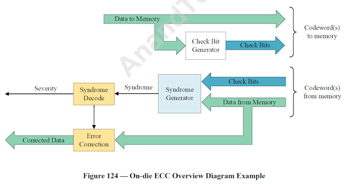
This decide is reproduced, with permission, from JEDEC doc JESD239, decide 124
Internally, the GDDR7 spec requires a minimal of 16 bits of parity data per 256 bits of client data (6.25%), with JEDEC giving an occasion implementation of a 9-bit single error correcting code (SEC) plus a 7-bit cyclic redundancy take a look at (CRC). Common, GDDR7 on-die ECC should have the power to proper 100% of 1-bit errors, and detect 100% of 2-bit errors – falling to 99.3% inside the unusual case of 3-bit errors. Particulars about memory errors will also be made accessible to the memory controller, by the use of what JEDEC phrases their on-die ECC transparency protocol. And whereas technically separate from ECC itself, GDDR7 moreover throws in a single different memory reliability operate with command deal with parity with command blocking (CAPARBLK), which is supposed to boost the integrity of the command deal with bus.
In some other case, whereas the inclusion of on-die ECC is just not extra more likely to have any additional of an impression on shopper video enjoying playing cards than its inclusion had for DDR5 memory and shopper platforms there, it stays to be seen what it is going to suggest for workstation and server video enjoying playing cards. The distributors there have used light ECC on prime of unprotected memory for quite a lot of generations now; presumably it is going to keep the case for GDDR7 enjoying playing cards as successfully, nonetheless the frequent use of soppy ECC makes points far more versatile than inside the CPU home.
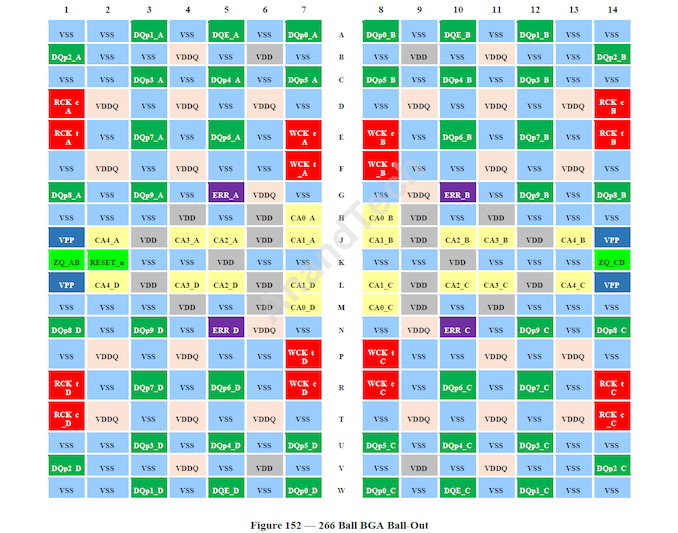
This decide is reproduced, with permission, from JEDEC doc JESD239, decide 152
Lastly, GDDR7 will also be introducing a set of various reliability-related choices, primarily related to serving to PAM3 operation. This incorporates core neutral LFSR (linear-feedback shift register) teaching patterns with eye masking and error counters. LFSR teaching patterns are used to verify and regulate the interface (to verify effectivity), eye masking evaluates signal prime quality, and error counters monitor the number of errors all through teaching.
Technical points aside, this week’s announcement incorporates statements of assist from all of the common avid gamers on both aspect of the isle, along with AMD and NVIDA, and the Micron/Samsung/SKhynix trifecta. It goes with out saying that every one occasions are desirous to getting to utilize or promote GDDR7 respectively, given the memory functionality and bandwidth enhancements it ought to ship – and significantly on this era the place one thing aimed on the AI market is selling like hotcakes.
No specific merchandise are being launched proper now, nonetheless with Samsung and Micron having beforehand launched their intentions to ship GDDR7 memory this 12 months, we should all the time see new memory (and new GPUs to pair it with) later this 12 months.
JEDEC necessities and publications are copyrighted by the JEDEC Steady State Know-how Affiliation. All rights reserved.


