


A Look into Efficiency & Effectivity
It’s been about two weeks since Google formally introduced their latest flagship units within the type of the Pixel 6, and Pixel 6 Professional. The 2 new Pixel telephones are inarguably Google’s largest shift ever because the Pixel sequence was launched, showcasing main adjustments in basically each facet of the units, sharing little or no in frequent with their predecessors in addition to the Pixel title. That includes model new shows, digicam methods, physique designs, and inner {hardware} at seemingly extraordinarily aggressive pricing, the telephones appear to be off to an especially good begin and aggressive positioning Google hasn’t had in a very long time.
One of many greatest adjustments, and most fascinating to our readers, is the truth that the Pixel 6 and Pixel 6 Professional come powered on by Google’s personal “Tensor” SoC. And it’s right here the place there’s fairly a little bit of confusion as to what precisely the Tensor is. Google explains that the Tensor is Google’s begin in a journey in direction of the search of enabling new sorts of workloads, which within the firm’s phrases, have been merely not attainable or achievable with “customary” service provider silicon options. Benefiting from Google analysis’s years of machine studying expertise, it’s a chip that’s closely centered in direction of ML as its main differentiating characteristic, and what’s stated to permit the Pixel 6 telephones to have most of the new distinctive characteristic unique to them.
At the moment, we’re giving the Tensor SoC a more in-depth look. This contains making an attempt to doc what precisely it’s composed of, showcasing the variations or similarities between different SoCs available in the market, and higher understanding what sort of IPs Google has built-in into the chip to make it distinctive and warrant calling it a Google SoC.
The Chip Provenance
Formally, per Google’s personal supplies, the Tensor is a Google SoC totally designed by the corporate. And whereas the general fact of this can differ primarily based in your definition of “design”, the chip follows a seemingly shut cooperation between Google and Samsung LSI, within the course of blurring the strains between a conventional {custom} design and semi-custom design-for-hire chips such AMD’s console APUs.
Beginning off on the very highest degree, we now have the precise title of the SoC. “Google Tensor” is sort of summary in that, in the meanwhile, the chip doesn’t have any specific mannequin quantity hooked up to it by way of official advertising. So whether or not the next-gen can be marketed “Tensor 2” or one thing else will stay to be seen. Internally, Google calls the chip the “GS101”, and whereas I’m not completely certain right here what GS stands for, it’s possible Google SoC or Google Silicon. For fairly a while now we’ve additionally heard the “Whitechapel” being reported, though I’ve seen no proof that this was a reference to the precise chip however within the very early phases.
On the silicon facet, the chip has one other mannequin quantity, with the SoC’s fused chip identification following Samsung’s Exynos naming scheme. Right here we discover the chip has an ID of “0x09845000”, which corresponds to what could be S5E9845 (Edit: It is really S5P9845). The newest Samsung LSI SoC, for reference, is the Exynos 2100, which is recognized because the S5E9840.
In fact, why would the Google SoC comply with an Exynos inner naming scheme? That’s the place we will start to see a number of the provenance of the design. It’s been extensively reported for a while that a couple of years again, Samsung opened up itself to semi-custom silicon design provides. A bit from August 2020 from ETNews appears to accurately describe Samsung’s marketing strategy and the way it pertains to the Google chip (in addition to describing a Cisco design win):
“Samsung Electronics is ready to fabricate semiconductor chips for Cisco Methods, which is the highest community gear maker on the planet, and Google and it’s answerable for the whole semiconductor manufacturing course of from design to manufacturing.[…]Samsung Electronics is presently engaged on a improvement section that entails chip design.[…]Samsung Electronics additionally obtained an order from Google relating to manufacturing of a couple of chip. It’s heard that Google requested a semiconductor that may go right into a sensor that may measure physique actions fairly than for processors that go into present IT units and an unprecedented software processor (AP).[…]Samsung Electronics is finishing up a special strategy because it seems to actively make the most of its applied sciences in chip design. Its technique is to supply “custom-made” applied sciences and options that its buyer wants even from a design stage and safe consignment manufacturing as properly.
What’s necessary right here is the latter description of the method – the place fairly than merely performing as a pure-play contract producer, Samsung is performing as a completely engaged celebration within the design of the silicon. This might very a lot be in comparison with an ASIC design service, with the exception being that Samsung can also be a service provider SoC vendor in addition to a producer for the silicon, one thing that’s fairly distinctive within the trade, and thus one thing of a particular scenario.
Having the chip in our palms now, in addition to having the open-source perception into the traits of it, we will begin breaking down what precisely the Google Tensor is:
| Google Tensor and Samsung Exynos 2100: Related However Totally different | ||
| SoC |
Google Tensor |
Exynos 2100 |
| CPU | 2x Cortex-X1 @ 2.80GHz 2x1024KB pL2 2x Cortex-A76 4x Cortex-A55 4MB sL3 |
1x Cortex-X1 @ 2.91GHz 1x512KB pL2 3x Cortex-A78 4x Cortex-A55 4MB sL3 |
| GPU | Mali G78 MP20 @ 848 MHz (shaders) 996 MHz (tiler / L2) |
Mali G78 MP14 @ 854 MHz |
| Reminiscence Controller |
4x 16-bit CH
@ 3200MHz LPDDR5 / 51.2GB/s 8MB System Cache |
|
| ISP | Hybrid Exynos + Google ISP | Full Exynos ISP Blocks + DSP |
| NPU | Google edgeTPU @ 1066MHz |
Exynos NPU @ 1352MHz |
| Media | Samsung Multi-Operate Codec
8K30 & 4K120 encode & H.265/HEVC, H.264, VP9 |
|
| Google “BigOcean” 4K60 AV1 Decode |
||
| Modem | Exynos Modem 5123 Exterior (LTE Class 24/18) |
Exynos Modem 5123 Built-in (LTE Class 24/18) |
| Mfc. Course of | Samsung 5nm (5LPE) |
|
Similar Blood Kind
Within the very fundamentals of what an SoC is, the Google Tensor carefully follows Samsung’s Exynos SoC sequence. Past the same old high-level blocks that folks have a tendency to speak about in an SoC, resembling CPUs, GPUs, NPUs, and different major traits, there’s the foundational blocks of a chip: these are the material blocks and IP, the clock administration structure, energy administration structure, and the design methodology of the implementing these items into precise silicon. Whereas on paper, a Samsung Exynos, a MediaTek Dimensity or a HiSilicon Kirin, or perhaps a Qualcomm Snapdragon (on the CPU facet) might need related designs by way of specs – with the identical high-level IP resembling Cortex CPU or Mali GPUs from Arm – the chips will nonetheless find yourself behaving and performing in a different way due to the underlying SoC structure may be very totally different.
Within the case of the Tensor, this “chassis” builds upon the IP Samsung makes use of on their Exynos SoCs, using the identical clock administration and energy administration structure. Going additional up within the IP hierarchy we discover extra similarities amongst high-level IP blocks, resembling reminiscence controllers, cloth IP, PHY IP for every kind of externally dealing with interfaces, and even the bigger IP practical blocks resembling ISP or media decoders/encoders. The enjoyable factor is that this stuff are actually publicly scrutinizeable, and might be in contrast 1:1 to different Exynos SoCs by way of their buildings.
This leads us to Google’s declare of the Tensor being their very own design – which is true to an extent, however how true that’s can differ primarily based in your definition of “design” and the way in-depth you wish to go along with that. Though the Tensor/GS101 builds upon Exynos foundational blocks and IPs – and sure was even built-in and taped-out by Samsung – the definition of the SoC is in Google’s management, as it’s their end-product. Whereas issues are similar to an Exynos 2100 on the subject of Tensor’s basis and lowest degree blocks, on the subject of the material and inner interconnects Google’s design is constructed in a different way. Which means that the spiderweb of how the assorted IP blocks work together with one another is totally different from Samsung’s personal SoC.
A sensible instance of that is how the CPU cores are built-in into the SoC. Whereas on the Exynos 2100 the CPU cluster seemingly lies very clearly in a smaller, extra outlined Samsung Coherent Interconnect, the Tensor SoC integrates the CPU clusters in a bigger CCI that seems to both be a really totally different configuration of the interconnect setup, or is a special IP altogether. In the meantime there are nonetheless some similarities, resembling having one predominant reminiscence visitors bus linked to the reminiscence controllers and one different lower-traffic “inner” bus for different IPs, which is how Exynos SoCs are inclined to separate issues. It needs to be attainable to reverse-engineer and map out the SoC in additional element, nevertheless that’s a time-consuming matter out of the scope of this piece.
The CPU Setup – 2x X1 + 2x A76 + 4x A55
Whereas we may go on and on speaking about SoC structure, let’s curtail that for now and leap into the extra seen and sensible variations of the Tenor SoC, beginning off with the CPU cluster.

Google’s CPU setup is sort of uncommon from different SoCs in that it contains a 2+2+4 configuration. Whereas this isn’t actually distinctive – Samsung had this exact same setup for the Exynos 9820 and Exynos 990 – the X1+A76+A55 configuration on the Tensor is presently distinctive available in the market. Most different distributors and implementations on the market have shifted over to a 1+3+4 large+mid+little CPU configurations.
On the Cortex-X1 facet, Google’s use of a pair of cores implies that, in principle, the efficiency of the chip with two heavy threads needs to be increased than every other Android SoC which solely have a single large massive efficiency core. The frequencies of the X1 pair are available in at 2.8GHz, barely decrease than the two.86GHz of the Snapdragon 888 and a couple of.91GHz of the Exynos 2100 X1 cores. Google geared up the cores with the complete 1MB of L2 cache, much like the S888 and double that of the E2100 configuration.
As for the center cores, Google has employed Cortex-A76 cores, which has been a scorching matter for dialogue. At first look, it’s seemingly a bit irrational contemplating each the Cortex-A77 and A78 supply increased efficiency and better power effectivity. The cores are clocked at 2.25GHz and include 256KB of L2. We haven’t obtained a transparent rationalization from Google as to why they used the A76, however I do assume it’s possible that on the time of design of the chip, Samsung didn’t have newer IP prepared for integration. The chip has been brewing for a while and whereas it does characteristic X1 cores, possibly it was too late within the course of to additionally shift over to newer center cores. I don’t assume there was a purposeful alternative of utilizing A76 cores as a substitute of A78, since as we’ll see in our efficiency benchmarks that the older design underperforms.
On the little cores, there are 4x A55 cores at 1.8GHz. In distinction to Samsung’s personal Exynos chips, Google has determined to equip the cores with 128KB of L2 caches fairly than simply 64KB, so that they’re extra consistent with the Snapdragon 888 configuration. One odder alternative from Google is that the L3 cache of the cluster is on the identical clock airplane because the A55 cores, which has latency and energy implications. It’s additionally at odds with the devoted L3 clock airplane we see on the Exynos 2100.
One other Fats Mali GPU: G78MP20 At Excessive Clocks
Earlier rumors concerning the SoC indicated that it could include a Mali-G78 era GPU, nevertheless we didn’t know the precise core depend or clocks of the design. Google has since confirmed the MP20 configuration, which is the second-largest Mali GPU configuration, behind solely the Kirin 9000 and its huge 24-core unit. I had initially theorized that Google was possible working the GPU at low frequencies to have the ability to optimize for power effectivity, solely to finish up fairly shocked to see that they’re nonetheless working the GPU at a peak clockspeed of 848MHz for the shader cores, and 996MHz for the tiler and L2. The Google Tensor, if I’m not mistaken, appears to be the primary confirmed G78 implementation really profiting from Arm’s break up clock airplane design of the G78, which permits the shared GPU cloth to run at the next frequency than the precise shader cores – and therefore why it has two frequencies.
The precise frequencies are extraordinarily excessive. The Exynos 2100’s G78MP14 already ran at 854MHz, and it was a chip which we deemed to have very excessive peak energy figures; however right here Google is including 42% extra cores and isn’t backing down on frequency. In order that’s very eye-brow elevating and regarding by way of peak GPU energy, issues which we’ll see materialize within the latter GPU analysis part.
LPDDR5, 8MB SLC Cache
The reminiscence controllers on the Google Tensor look like the identical as on the Exynos 2100, supporting LPDDR5 in a 4x 16-bit channel configuration for a complete peak theoretical bandwidth of 51.2GB/s.
Google additionally built-in 8MB of system cache, and for me it isn’t precisely clear if this is similar IP Samsung makes use of on the Exynos 2100. Seemingly they’re each 8MB, however I’m leaning in direction of saying that it’s a special IP, or on the very least a special model of the IP, as there are some actual variations in the best way it’s architected and the way it behaves.
Google right here makes very intensive utilization of the SLC for enhancing the efficiency of the SoC blocks, together with their very own {custom} blocks. The SLC permits itself to be partitioned and to dedicate SRAM areas to specific IP blocks on the SoC, giving them unique entry to all or components of the cache in various use-case conditions.
A Customized Hybrid ISP Pipeline
Normally when individuals or corporations speak about SoC ISPs, these are all the time depicted as being a single monolithic IP block. In actuality what we name an “ISP” is a mixture of various specialised IP blocks, every dealing with totally different duties in what we name the imaging pipeline. The Google Tensor right here is fascinating in that it takes bits and items of what Samsung makes use of on their Exynos chips, and in addition integrates {custom} Google-developed blocks into the pipeline – one thing Google really talked about of their presentation of the SoC.
The imaging system makes use of IP blocks that correspond to an Exynos imaging pipeline, resembling pixel section detection processing models, distinction autofocus processing models, picture scalers, distortion correction processing blocks and view-dependent occlusion texture perform processing blocks. What’s missing right here is that another processing blocks are lacking, which I think about are associated to extra post-processing computation blocks that Samsung makes use of.
The Google developed IP blocks within the ISP chain appear to be their very own 3AA IP (Auto-Publicity, Auto-White Steadiness, Auto-Focus), in addition to a {custom} pair of temporal noise-reduction IP blocks which can be in a position to align and merge pictures. These are possible the {custom} blocks that Google was speaking about when saying that they’ve developed blocks which assist speed up the type of picture processing that they make use of as a part of the Pixel lineup’s computational pictures, and inarguably signify essential components of the picture processing pipeline.
Google’s edgeTPU – What Makes the Tensor a Tensor
By now, it’s been fairly clear that the large central speaking level of the Google Tensor has been its TPU – or its Tensor Processing Unit. The TPU is, as its title implies, a {custom} Google developed-IP block that the corporate has been engaged on for a couple of years now. Till now, Google simply referred to as it the TPU contained in the Tensor SoC, however on the driver degree the corporate calls the block their “edgeTPU”. That is fairly fascinating as alerts that the block is said to the ASIC “Edge TPU” that Google had introduced again in 2018. The discrete chip had been marketed at 4 TOPs of processing energy in 2 Watts of energy, and whereas Google doesn’t promote any efficiency metrics on the TPU contained in the Tensor, there are entries showcasing the block goes as much as 5W of energy. So if the 2 are certainly associated, then given the numerous course of node benefits and general a lot newer IP, the efficiency figures of the Tensor TPU (sic) needs to be extraordinarily important.
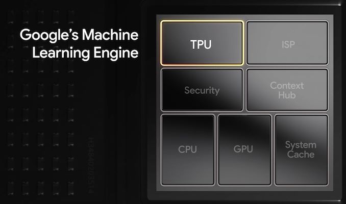
The block may be very a lot the satisfaction of Google’s silicon workforce, telling us that it’s utilizing the newest structure for ML processing that’s been optimized for the best way Google’s R&D groups run machine studying inside the firm, and guarantees to permit for opening up the type of new and distinctive use-cases that have been the primary purpose for making a {custom} SoC within the first place. We’ll go into the product-side use-cases in a extra Pixel centered evaluate afterward, however the efficiency metrics of the TPU do look like spectacular.
The TPU block additionally appears to return with some kind of block that Google calls “GSA”. That is simply hypothesis on my half right here primarily based on the drivers, however this appears to be some kind of management block that’s accountable for working the TPU firmware, and I feel comprises a quad-core Cortex-A32 CPU setup.
Media Encoders, Different Stuff
On the media encoder facet, the Tensor SoC makes use of each Samsung’s personal Multi-Operate Codec IP block (which is similar to what’s used on the Exynos sequence) in addition to what seems to be a Google IP block that’s devoted to AV1 decoding. Now it is a bit bizarre, as Samsung does promote the Exynos 2100 as having AV1 decode talents, and that performance does appear to be there within the kernel drivers. Nevertheless on the Galaxy S21 sequence this performance was by no means carried out on the Android framework degree. I’ve no good rationalization right here as to why – possibly the IP isn’t working accurately with AV1.
The Google IP block, which the corporate calls “BigOcean”, is a devoted AV1 decoder, and this does really expose AV1 decoding potential to the Android framework. The very bizarre factor right here is that each one it does is AV1 – each different encoding and decoding of different codecs is left over to the Samsung MFC. It’s an fascinating scenario and I’m left to marvel the place issues evolve within the next-gen SoC.
Different variations for the Tensor SoC are for instance the audio subsystem. Samsung’s SoC low-power audio decoding subsystem is thrown out in favor of Google’s personal block design, I didn’t dwell an excessive amount of into it however typically each blocks have the identical job of permitting low-power audio playback without having to get up massive components of the SoC. I feel this block (or the GSA) can also be accountable because the always-on context-hub for sensor knowledge aggregation, with the Tensor right here utilizing Google’s IP and means of doing issues versus the Exynos variant of the identical block.
Google additionally employs a set perform {hardware} reminiscence compressor within the type of a block referred to as Emerald Hill, which supplies LZ77 compression acceleration for reminiscence pages, and might in flip be used to speed up ZRAM offloading in swap. I’m unsure if the Pixels are presently working this out of the field, however ought to be capable to be confirmed by seeing “lz77eh” in /sys/block/zram0/comp_algorithm , if someone is ready to learn that out. As an anecdote, way back to 5 years in the past Samsung built-in related {hardware} compression IP blocks into their SoCs for the exact same job, however for some motive these have been by no means enabled for delivery units. Possibly the power effectivity didn’t pan out as they thought it could.
Exterior Exynos Modem – First non-Qualcomm mmWave Telephones?
Because it’s a telephone SoC, naturally the Tensor wants some kind of mobile connectivity. That is one other space the place Google is counting on Samsung, utilizing the corporate’s Exynos Modem 5123. However, not like the Exynos 2100 and its built-in modem, the Tensor makes use of a discrete exterior variant. As to why it’s discrete, it’s possible that with the huge GPU, bigger CPU setup (two X1’s with full 1MB L2’s), and unknown measurement of the TPU, that the Tensor chip is sort of massive even in relation to the Exynos 2100.
Supply: PBKreviews
One other principle on my facet is that Google would by some means nonetheless be tied to Qualcomm for US networks – both for CDMA or mmWave 5G connectivity. Surprisingly, it appears this isn’t the case, because the Pixel 6 sequence ships with the Exynos modem throughout the globe. That makes the Pixel 6 household notably fascinating, as plainly that is the primary non-Qualcomm mmWave implementation on the market. For reference, Samsung had talked about their mmWave RFICs and antenna modules again in 2019, saying there have been plans for 2020 units. Whether or not that meant designs beginning in 2020 (which the Pixel 6 sequence could be) or industrial availability wasn’t clear on the time, however plainly these are the primary industrial telephones with the answer. I don’t count on to have mmWave protection right here for myself for an additional few years, however third-party stories showcase the telephone reaching as much as 3200Mbps whereas different field-tests exhibiting round half of the sensible speeds of Qualcomm units. I hope extra individuals within the subsequent weeks and months could have the chance to dive deeper into the modem’s efficiency traits.
Semi-Customized Appears Apt
Total, the Google Tensor finally ends up being virtually precisely what we anticipated the chip to be, from the earliest stories of a collaboration between Google and Samsung. Is it a Google chip? Sure, they designed it within the sense that they outlined it, whereas additionally creating fairly a couple of Google-unique blocks which can be integral to the chip’s differentiation. Is it a Samsung Exynos chip? Additionally sure, from a extra foundational SoC structure degree, the Tensor has a fantastic deal in frequent with Samsung’s Exynos designs. In a number of areas of the Tensor there are architectural and behavioral parts which can be distinctive to Samsung designs, and aren’t discovered anyplace else. To that finish, calling the Google Tensor a semi-custom design appears completely apt for what it’s. That being, stated, let’s see how the Tensor behaves – and the place it lands by way of efficiency and effectivity.

 and Pixel 5 Later This Yr")
